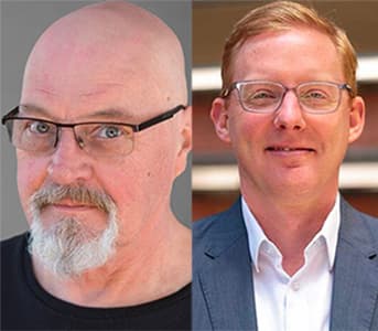
Pat Gelsinger Bets on Light-Based Lithography to Revive Moore's Law
The former Intel CEO explains why advanced chip-printing technology—not processor design—holds the key to semiconductor breakthroughs.

Former Intel chief targets chip manufacturing's hardest problem
Pat Gelsinger spent 100 days evaluating his next move after leaving Intel in late 2024. By March, the longtime semiconductor executive had chosen venture capital over private equity, government roles, and another CEO position—specifically to work on what he calls the semiconductor industry's "hardest problem."
Gelsinger joined Playground Capital as general partner, taking a board seat at xLight, a portfolio company developing advanced lithography techniques that recently secured U.S. government investment. His focus: reawakening Moore's Law through breakthroughs in how chips are manufactured, not just how they're designed.
Why it matters
The semiconductor industry now expects to reach $1 trillion in revenue next year—six years ahead of 2024 projections—driven entirely by AI demand. But continued progress depends on solving fundamental physics challenges in chip manufacturing. Gelsinger's bet on lithography represents a strategic wager that manufacturing innovation, rather than novel processor architectures, will determine which companies capture that explosive growth.
Light wavelengths as the bottleneck
Current leading-edge lithography from Dutch manufacturer ASML uses 13.5-nanometer wavelength light to etch chip features. Gelsinger believes free-electron lasers could push this to 5-, 4-, or even 2-nanometer wavelengths, enabling far denser transistor packing.
"If we solve light, that is the hardest problem," Gelsinger told WIRED in an interview at the RAISE Summit conference in Paris. He emphasized that xLight's technology would complement rather than compete with ASML, initially connecting new light sources to existing manufacturing equipment.
All emerging semiconductor technologies—new material structures, superconducting circuits, ferroelectric materials—still require lithography advances, according to Gelsinger. "It's always been the center of semiconductors," he said.
Deep tech investing after the AI boom
Gelsinger's shift to venture capital reflects broader industry movement toward deep tech investment as AI reshapes software markets. He argues most venture firms "have forgotten how to do deep tech—how to pick the winners and losers."
Playground Capital's investment team comprises engineers, PhDs, and professors who conduct rigorous technical diligence. Gelsinger's process focuses on identifying the best team working on a given problem, noting that breakthrough ideas typically attract two or three competing startups rather than single "dodo bird" companies.
Beyond lithography, Gelsinger is backing companies working on memory architecture, energy efficiency, and power distribution. He believes AI hardware innovations could deliver 10 to 100 times better performance than current GPUs, translating directly to energy efficiency gains the industry desperately needs.
Energy and regulation challenges
Gelsinger identified energy capacity as a critical bottleneck, noting U.S. energy expansion remained in low single digits over the past decade. "In a digital AI age, energy capacity is economic capacity," he said. Playground portfolio company Alva Energy focuses on nuclear power upgrades as a faster path than new construction.
On AI regulation, Gelsinger advocated for model integrity requirements—either industry-led or government-mandated—including transparency about training data, vigorous benchmarking, and security testing. "We're figuring it out in real time, because things are moving so rapidly," he acknowledged.
These details were first reported by WIRED.
This is an original analysis by the Omega editorial team. Source reporting: WIRED.
Want systems like this working for your business?
Book a Call