Kepler Computing Raises $468M to Bypass EUV Lithography
The stealth startup claims its ferroelectric materials and 3D stacking can boost memory density without the industry's most expensive manufacturing equipment.
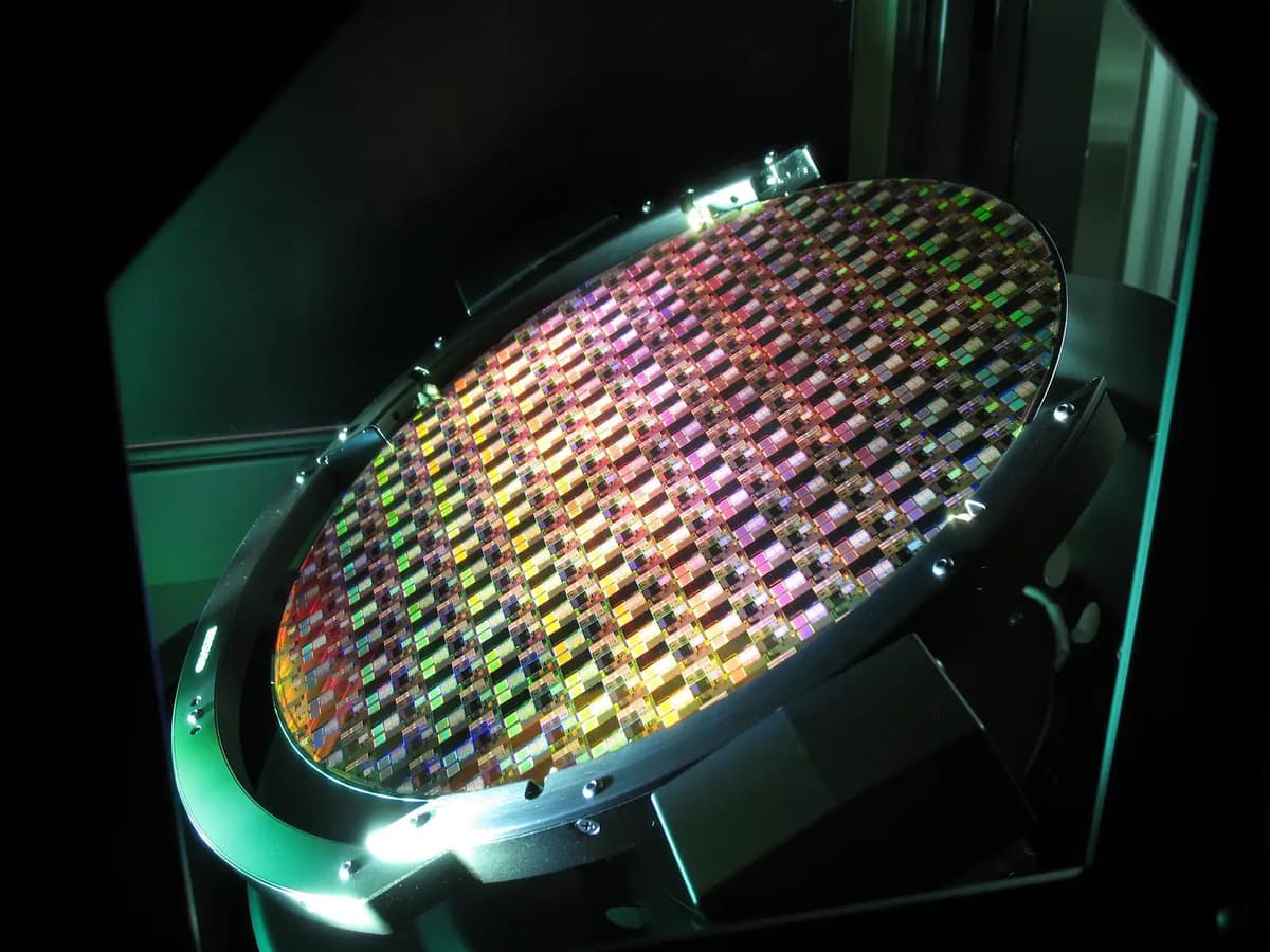
A San Jose chip startup has emerged from seven years in stealth mode with a bold claim: it can produce denser memory chips without the semiconductor industry's most expensive manufacturing tool.
Kepler Computing announced it has raised $468 million from investors including GlobalFoundries, Intel Capital, AMD Ventures, Baillie Gifford, and Bill Gates through his Gates Frontier fund. The company says its approach to high-bandwidth memory (HBM) and static random-access memory (SRAM) can increase chip density while working with existing fabrication facilities—no extreme ultraviolet lithography required.
Why it matters
The global memory shortage has exposed a fundamental constraint in semiconductor manufacturing: building new fabs costs $20 billion to $40 billion and takes years to complete. If Kepler can deliver on its promise to retrofit existing facilities in eight months instead of the typical 24, it could provide a faster path to meeting surging AI-driven demand for HBM. The approach also sidesteps the EUV bottleneck that has made advanced chipmaking prohibitively expensive for all but the largest players.
A materials breakthrough
Kepler's technology rests on two innovations, according to details first reported by WIRED. For HBM, the company developed a 3D manufacturing technique that stacks more memory within the same physical footprint, reducing the distance data must travel between compute and memory. The goal is to match SRAM's energy efficiency while maintaining HBM's large capacity.
For SRAM, Kepler uses ferroelectric materials that read and write data at lower voltages than conventional semiconductors. Chief Technology Officer Sasi Manipatruni told WIRED the team tested 35 composite materials before settling on a formulation that works with the ferroelectric approach. The company claims this combination achieves density equivalent to 2-nanometer or 3-nanometer chips without EUV equipment.
The contamination challenge
GlobalFoundries, which invested $50 million and is manufacturing partner, acknowledged one significant hurdle: Kepler's composite material includes iron, which can contaminate production equipment. "Iron is a tough contaminant to introduce into a production facility," Ed Kaste, senior vice president of GlobalFoundries' CMOS business, told WIRED. The solution requires dedicated equipment or full encapsulation to prevent cross-contamination.
Kepler has been testing its technology at GlobalFoundries facilities in Singapore and Burlington, Vermont, producing chips on approximately 2,000 wafers to date. The U.S. Department of Commerce committed up to $245 million in July to support domestic development of the technology.
Long road to production
The company plans to ship first HBM samples later this year, ramp Singapore production in 2026, and begin U.S. manufacturing in 2028. CEO Debo Olaosebikan told WIRED the shift in focus came after ChatGPT's 2022 launch sparked explosive HBM demand.
Scale remains the critical test. Kaste said the fundamental breakthroughs have occurred, but success requires "getting good results on thousands of wafers and millions of devices." Industry observers note that proving a new manufacturing method and meeting historic demand levels are entirely different challenges.
The details were first reported by WIRED.
This is an original analysis by the Omega editorial team. Source reporting: WIRED.
Want systems like this working for your business?
Book a Call